Process engineers and integrators can use virtual process modeling to test alternative process schemes and architectures without relying on wafer-based testing. One important aspect of building an accurate process model […]
CoventorMP® 1.3 Enhances Device Construction, Modeling Capabilities and Simulation Performance to Accelerate the Development of Next-Generation MEMS Technology Fremont, CA—JULY 17, 2020 – Coventor®, a Lam® Research Company, the global […]
Lam Research® is one of the top equipment suppliers in the semiconductor ecosystem. As a trusted, collaborative partner to the world’s leading semiconductor companies, Lam Research is a fundamental enabler […]
UNDERSTANDING THE BENEFITS AND CHALLENGES OF A NEW, NEXT-GENERATION SEMICONDUCTOR ARCHITECTURE In our November 2019 blog [1], we discussed using virtual fabrication (SEMulator3D®) to benchmark different process integration options for […]
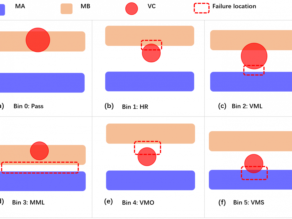
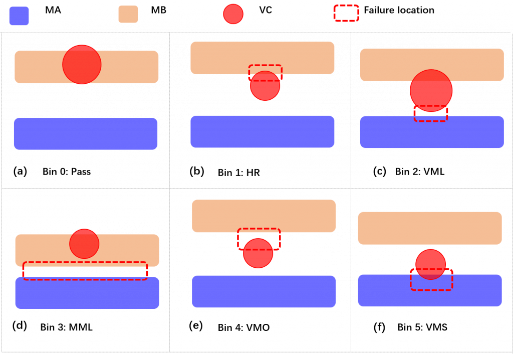
Using failure bin classification, yield prediction and process window optimization to predict and enhance yield Device yield is highly dependent upon proper process targeting and variation control of fabrication steps, […]
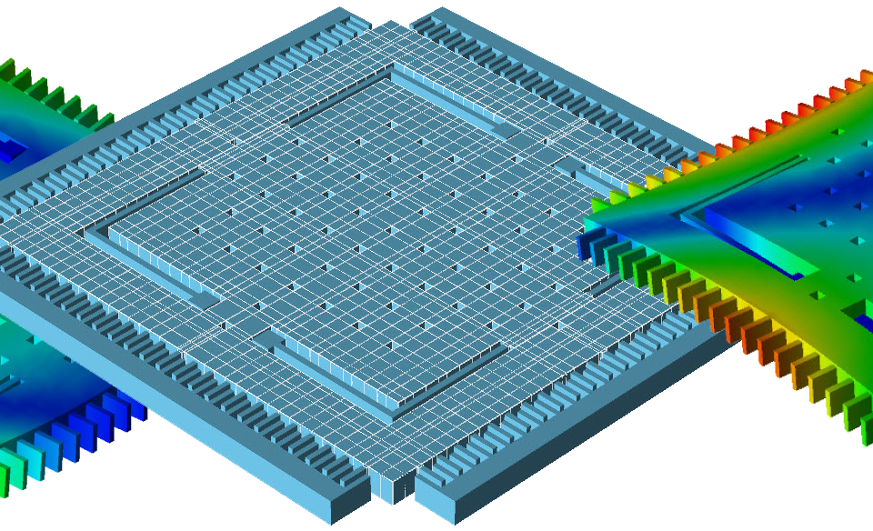
The IEEE MEMS conference was held in Vancouver during January 2020. We attended the conference to meet with our customers and to see what new developments are being made in […]
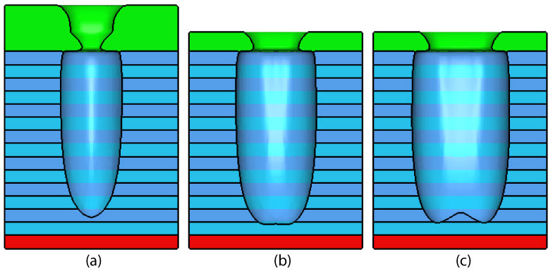
Via patterning at advanced nodes requires extremely low critical dimension (CD) values, typically below 30nm. Controlling these dimensions is a serious challenge, since there are many inherent sources of variation […]
In MEMS technology development, it is always exciting to see the next technology frontier, the border of the known and the unknown. Talent and hard work (along with ingenuity) can […]
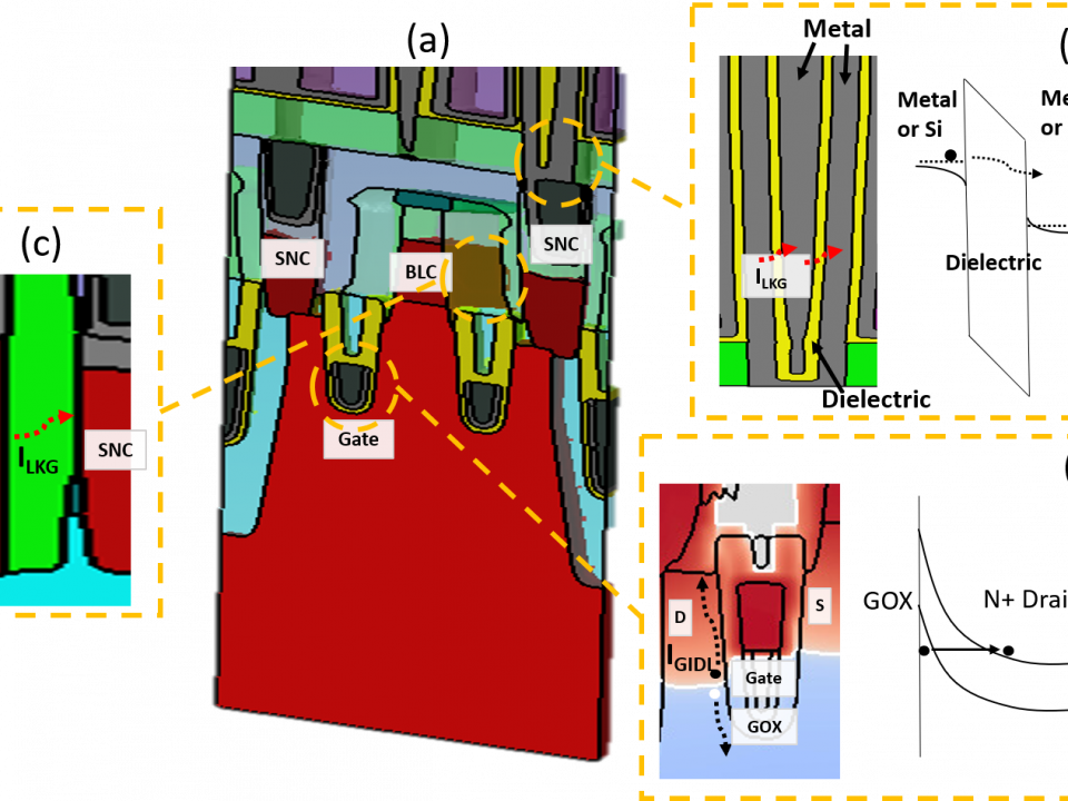
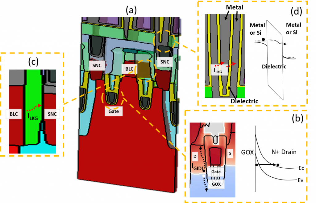
Leakage current has been a leading cause of device failure in DRAM design, starting with the 20nm technology node. Problems with leakage current in DRAM design can lead to reliability […]
Semiconductor process engineers would love to develop successful process recipes without the guesswork of repeated wafer testing. Unfortunately, developing a successful process can’t be done without some work. This blog […]


