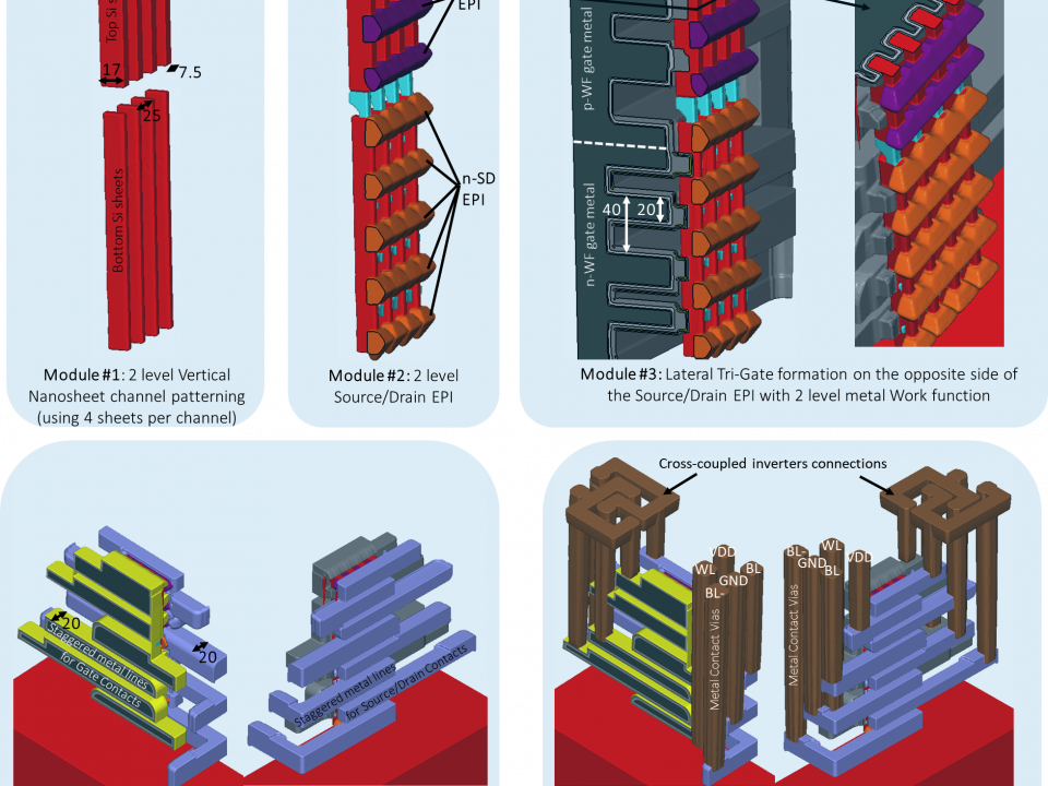
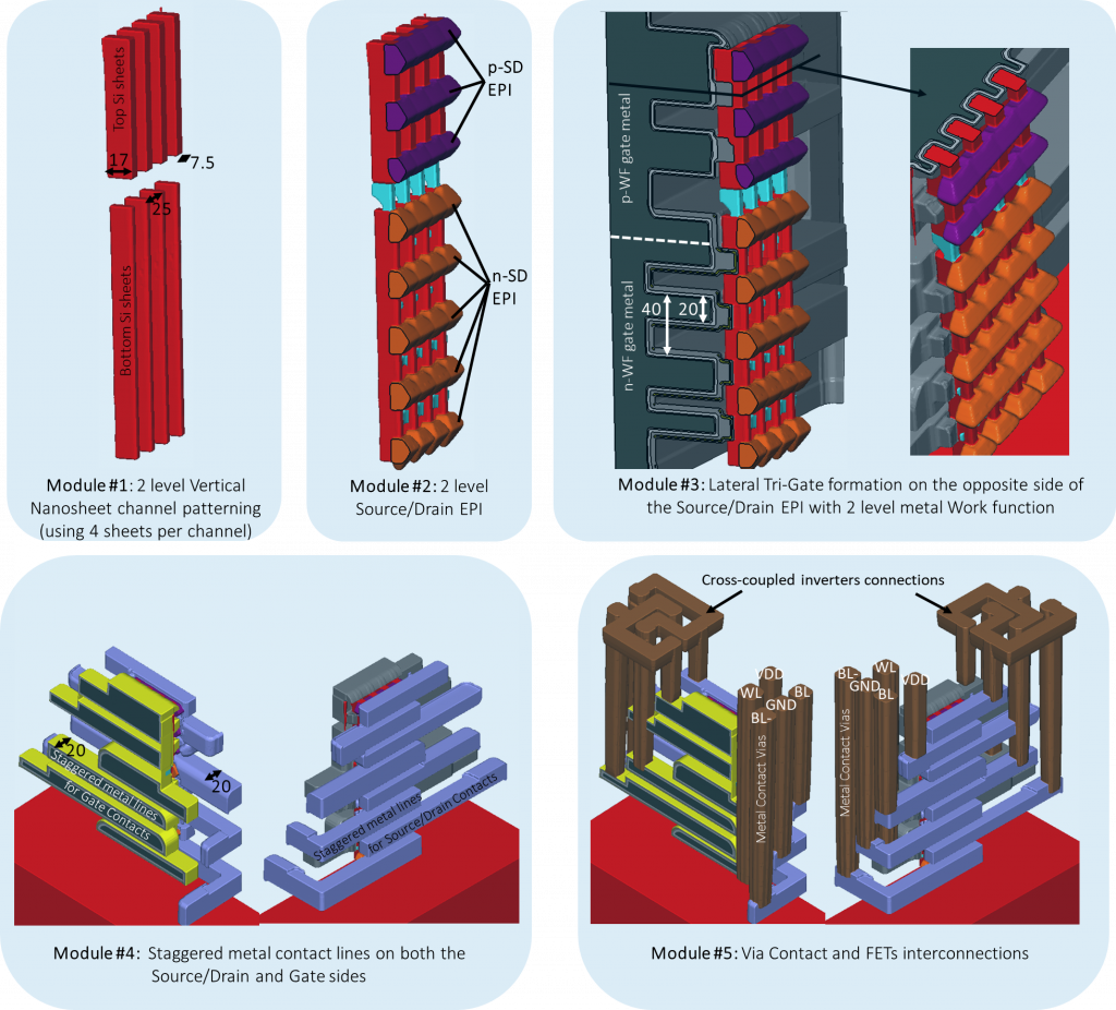
Static Random-Access Memory (SRAM) has been a key element for logic circuitry since the early age of the semiconductor industry. The SRAM cell usually consists of six transistors connected to […]
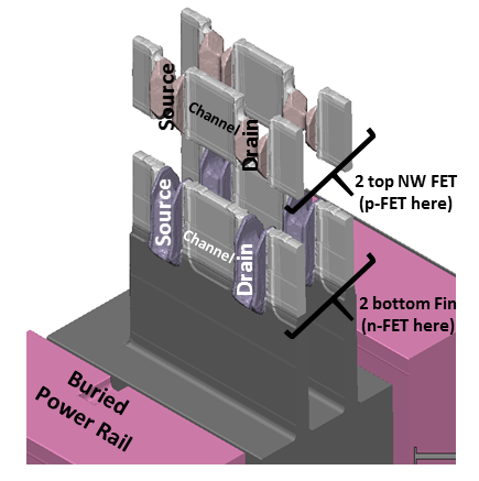
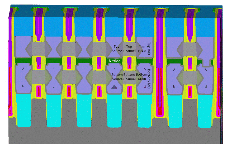
UNDERSTANDING THE BENEFITS AND CHALLENGES OF A NEW, NEXT-GENERATION SEMICONDUCTOR ARCHITECTURE In our November 2019 blog [1], we discussed using virtual fabrication (SEMulator3D®) to benchmark different process integration options for […]
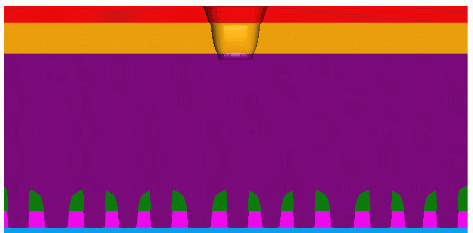
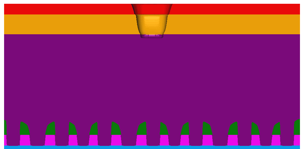
Via patterning at advanced nodes requires extremely low critical dimension (CD) values, typically below 30nm. Controlling these dimensions is a serious challenge, since there are many inherent sources of variation […]
Decision making is a critical step in semiconductor technology development. R&D semiconductor engineers must consider different design and process options early in the development of a next-generation technology. Established techniques […]
To ensure success in semiconductor technology development, process engineers must set the allowed ranges for wafer process parameters. Variability must be controlled, so that final fabricated devices meet required specifications. […]
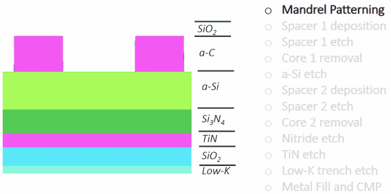
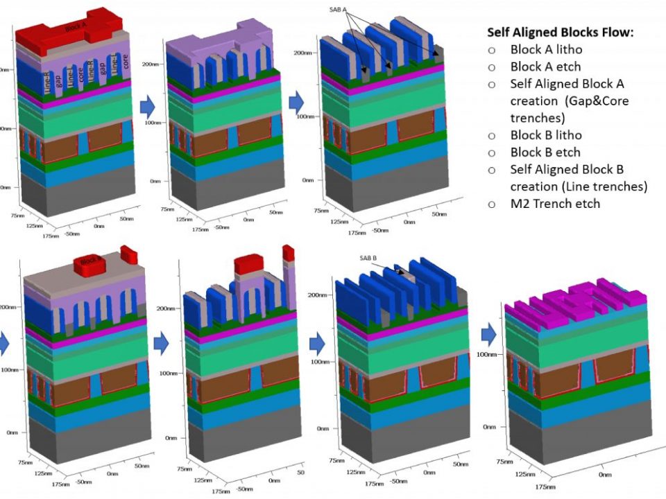
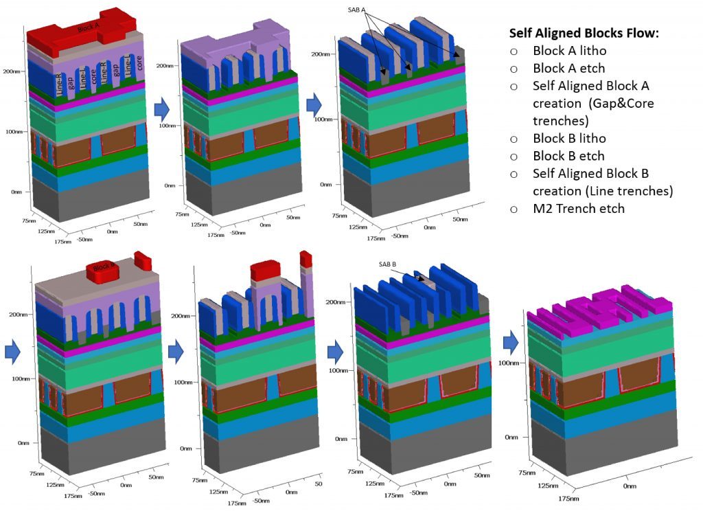
Advanced logic scaling has created some difficult technical challenges, including a requirement for highly dense patterning. Imec recently confronted this challenge, by working toward the use of Metal 2 (M2) […]
Engineering decisions are always data-driven. As scientists, we only believe in facts and not in intuition or feelings. At the manufacturing stage, the semiconductor industry is eager to provide data […]
