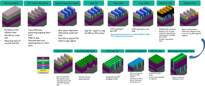
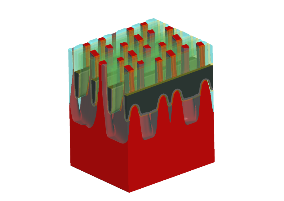
Introduction As we approach the 1.5nm node and beyond, new BEOL device integration challenges will be presented. These challenges include the need for smaller metal pitches, along with support for […]
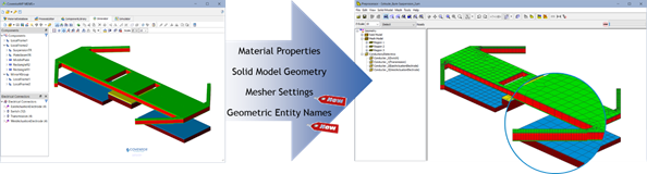
What is 3D Solid Modeling? You’ve certainly heard of “3D Solid Modeling”. The term first originated in the verification engineering community and has now become nearly ubiquitous. Mainstream industries like […]
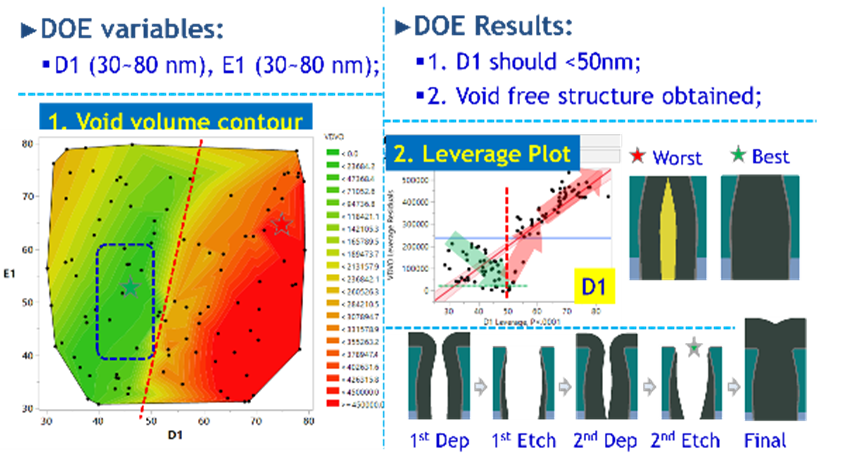
Design of Experiments (DOE) is a powerful concept in semiconductor engineering research and development. DOEs are sets of experiments used to explore the sensitivity of experimental variables and their effect […]
In any given year, we expect about 16 major earthquakes worldwide, 15 of which are in the magnitude 7 range and one in the magnitude 8.0 range or greater [1]. […]
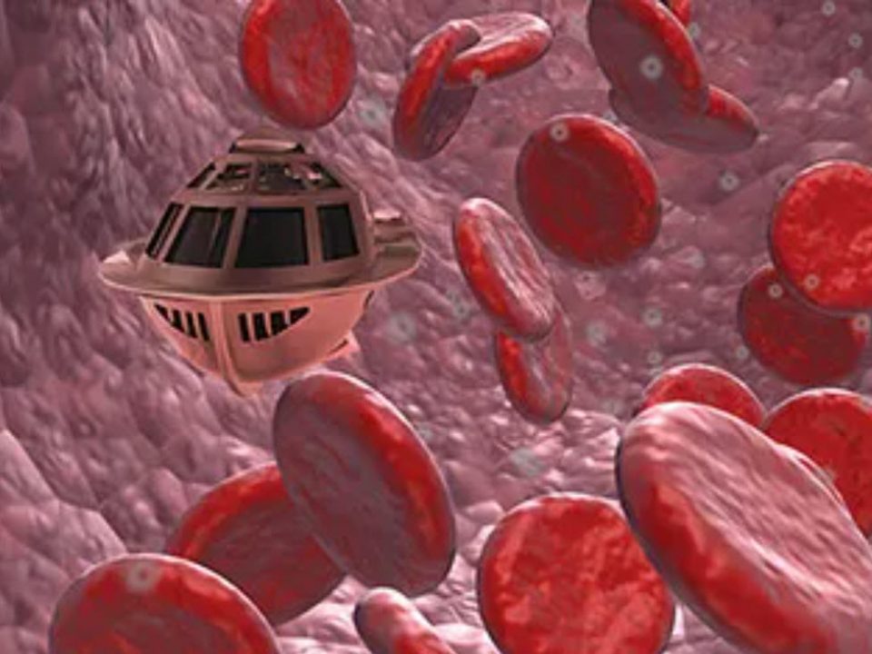
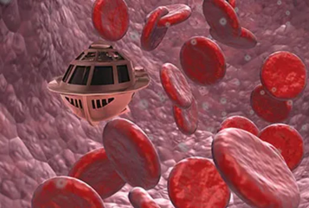
When I was a small child, I remember watching a 1966 American sci-fi adventure movie called “Fantastic Voyage” (the Korean title was “Micro Squad”) on an old black-and-white TV. The […]
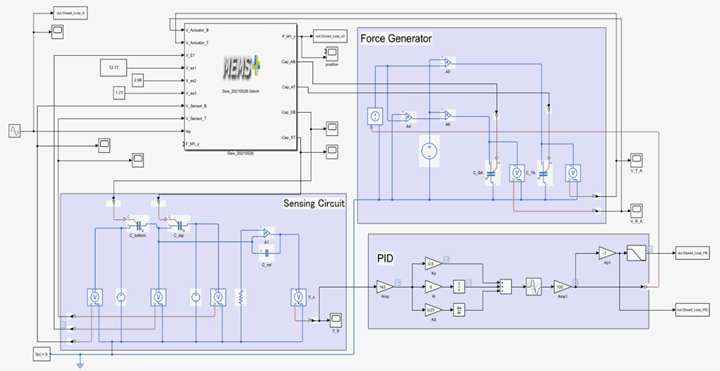
A digital twin is a digital representation of a real-world item, and includes software objects or models that represents these real-world items. In MEMS product development, digital twins (or software […]
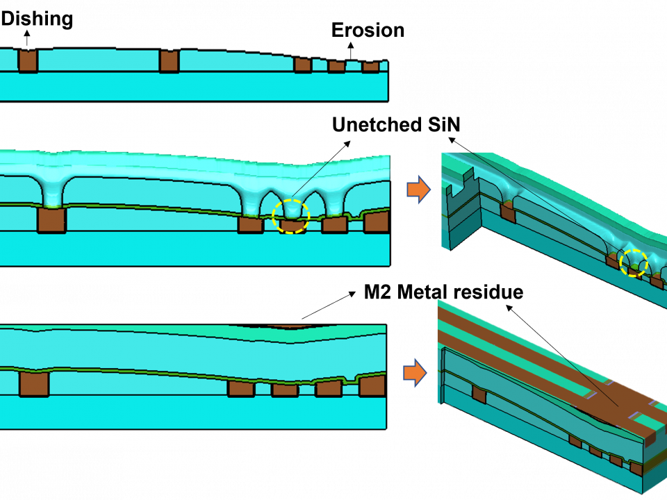
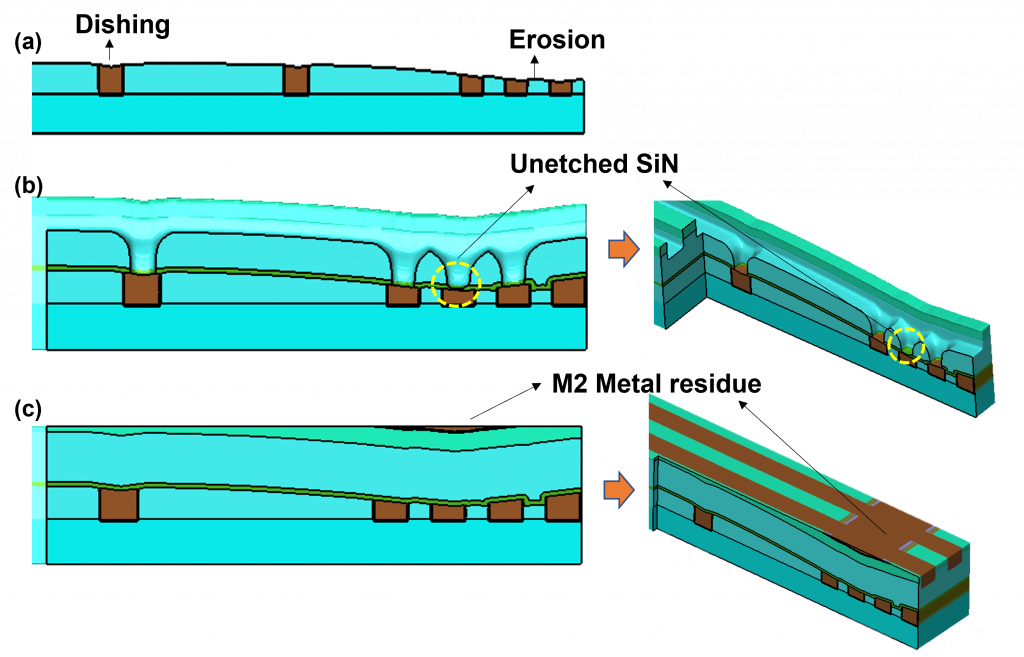
CMP (Chemical mechanical planarization) is required during semiconductor processing of many memory and logic devices. CMP is used to create planar surfaces and achieve uniform layer thickness during semiconductor manufacturing, […]
When evaluating shrinking metal linewidths in advanced semiconductor devices, bulk resistivity is not the sole materials property for deriving electrical resistance. At smaller line dimensions, local resistivity is dominated by […]
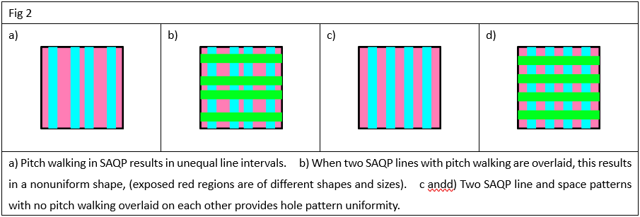
Despite the growing interest in EUV lithography, self-aligned quadruple patterning (SAQP) still holds many technical advantages in pattern consistency, simplicity, and cost. This is particularly true for very simple and […]
We are very pleased to announce the release of our latest MEMS design software, CoventorMP® 2.0! With the new release, automated parametric design variation for simulation in both MEMS+® and […]
